- 您现在的位置:买卖IC网 > Sheet目录1992 > CY28551LFXC (Silicon Laboratories Inc)IC CLOCK INTEL/AMD SIS VIA 64QFN
CY28551
....................Document #: 001-05675 Rev. *C Page 19 of 28
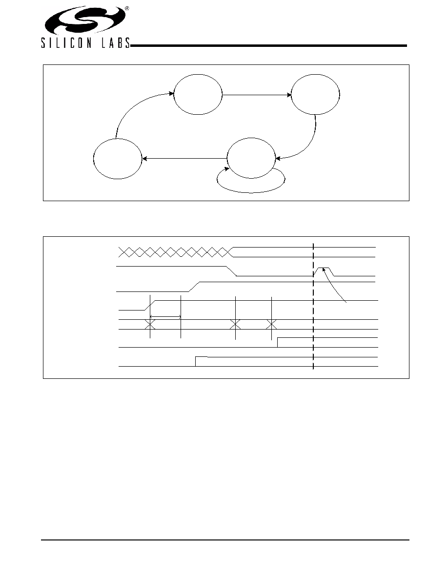
VTT_PWRGD# = Low
Delay >
0.25 ms
S1
Power Off
S0
VDD_A = 2.0V
Sample
Inputs straps
S2
Normal
Operation
Wait for <1.8 ms
Enable Outputs
S3
VTT_PWRGD# = toggle
VDD_A = off
Figure 10. VTT_PWRGD# Timing Diagram
FS_[D:A]
VTT_PWRGD#
PWRGD_VRM
VDD Clock Gen
Clock State
Clock Outputs
Clock VCO
0.2-0.3 ms
Delay
State 0
State 2
State 3
Wait for
VTT_PWRGD#
Sample Sels
Off
On
State 1
Device is not affected,
VTT_PWRGD# is ignored
Figure 11. VTT_PWRGD# Timing Diagram
发布紧急采购,3分钟左右您将得到回复。
相关PDF资料
CY2SSTV855ZXI
IC CLOCK DIFFDRV PLL DDR 28TSSOP
CY2SSTV857ZXI-27
IC CLK DDR266/333BUF1:10 48TSSOP
CY2SSTV857ZXI-32
IC CLK DDR266/333BUF1:10 48TSSOP
CY505YC64DT
IC CLK CK505 BROADWATER 64TSSOP
CYW150OXC
IC CLOCK 440BX AGP 56SSOP
CYW173SXC
IC CLK GEN TAPE DRV 4CH 16SOIC
CYW305OXC
IC CLOCK W305 SOLANO 56SSOP
DAC5674IPHPG4
IC DAC 14BIT 400MSPS 48-HTQFP
相关代理商/技术参数
CY28551LFXC-3
功能描述:时钟发生器及支持产品 Universal System Clk Intel AMD SiS Via RoHS:否 制造商:Silicon Labs 类型:Clock Generators 最大输入频率:14.318 MHz 最大输出频率:166 MHz 输出端数量:16 占空比 - 最大:55 % 工作电源电压:3.3 V 工作电源电流:1 mA 最大工作温度:+ 85 C 安装风格:SMD/SMT 封装 / 箱体:QFN-56
CY28551LFXC-3T
功能描述:时钟发生器及支持产品 Universal System Clk Intel AMD SiS Via RoHS:否 制造商:Silicon Labs 类型:Clock Generators 最大输入频率:14.318 MHz 最大输出频率:166 MHz 输出端数量:16 占空比 - 最大:55 % 工作电源电压:3.3 V 工作电源电流:1 mA 最大工作温度:+ 85 C 安装风格:SMD/SMT 封装 / 箱体:QFN-56
CY28551LFXCT
功能描述:时钟发生器及支持产品 Universal System Clk Intel AMD SiS Via RoHS:否 制造商:Silicon Labs 类型:Clock Generators 最大输入频率:14.318 MHz 最大输出频率:166 MHz 输出端数量:16 占空比 - 最大:55 % 工作电源电压:3.3 V 工作电源电流:1 mA 最大工作温度:+ 85 C 安装风格:SMD/SMT 封装 / 箱体:QFN-56
CY2862-000
制造商:TE Connectivity 功能描述:82A0111-4-9-G110
CY2863-000
制造商:TE Connectivity 功能描述:82A0111-8-9-G110 - Bulk
CY28800
制造商:CYPRESS 制造商全称:Cypress Semiconductor 功能描述:100-MHz Differential Buffer for PCI Express and SATA
CY28800OXC
功能描述:时钟缓冲器 PCI Express & Sata Diff Buffer 100MHz RoHS:否 制造商:Texas Instruments 输出端数量:5 最大输入频率:40 MHz 传播延迟(最大值): 电源电压-最大:3.45 V 电源电压-最小:2.375 V 最大功率耗散: 最大工作温度:+ 85 C 最小工作温度:- 40 C 封装 / 箱体:LLP-24 封装:Reel
CY28800OXCT
功能描述:时钟缓冲器 PCI Express & Sata Diff Buffer 100MHz RoHS:否 制造商:Texas Instruments 输出端数量:5 最大输入频率:40 MHz 传播延迟(最大值): 电源电压-最大:3.45 V 电源电压-最小:2.375 V 最大功率耗散: 最大工作温度:+ 85 C 最小工作温度:- 40 C 封装 / 箱体:LLP-24 封装:Reel